K4A8G085WC-BCTD Samsung 8Gb DDR4 SDRAM
Samsung K4A8G085WC-BCTD is an 8Gb x8 DDR4 SDRAM component. Samsung lists this exact ordering family in its DDR4 component guide for PC/server memory configurations.
Availability, quantity and lead time are confirmed in your quotation.
K4A8G085WC-BCTD Specifications
Basic specifications
- Manufacturer
- Samsung
- Complete part number
- K4A8G085WC-BCTD
- Memory type
- DDR4 SDRAM
- Component density
- 8Gb
- Organization
- 1G x8
- Data bus width
- x8
Speed & electrical
- TD speed designation
- 2666 MT/sOrdering-code rating; full timing modes require the matching specification.
- Clock
- 1333 MHz
- VDD / VDDQ
- 1.2 V
- Native CL / tRCD / tRP
- 19-19-19Native DDR4-2666; see Technical notes for full limits and modes.
- VDD / VDDQ operating range
- 1.14–1.26 VRails must track, with VDDQ ≤ VDD.
- VPP
- 2.5 VOperating range: 2.375–2.750 V.
Package & temperature
- Package
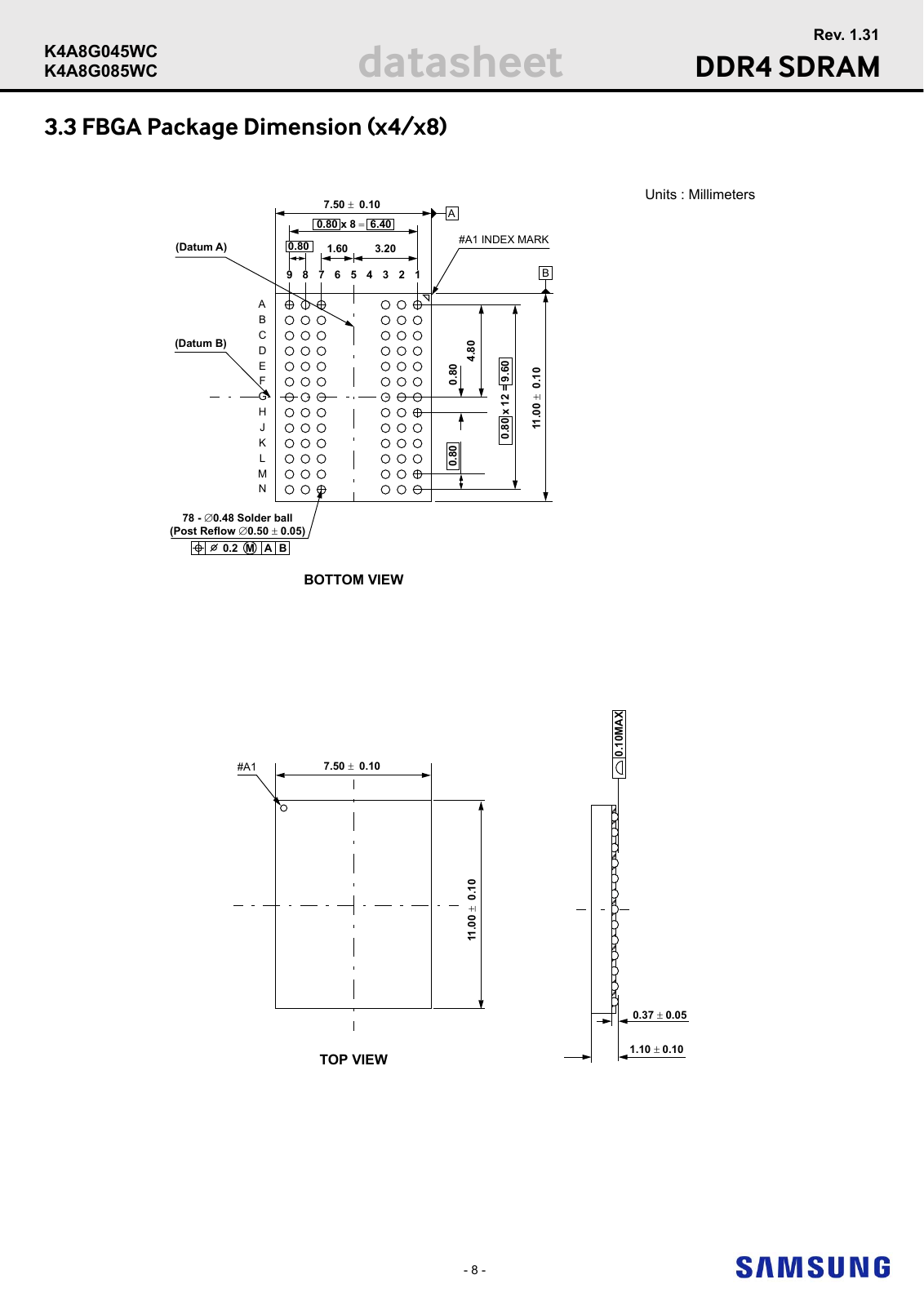
- 78-ball FBGA
- Temperature option
- Commercial (C)
- Body size
- 7.50 ±0.10 × 11.00 ±0.10 mmW × L; manufacturer tolerances.
- Overall height
- 1.10 ±0.10 mm
- Ball pitch
- 0.80 mmDimensioned on both axes.
- Normal case range
- 0 to +85 °CMeasured at top center of the case.
- Extended case range
- >85 to +95 °CAdditional refresh and self-refresh conditions apply.
Technical notes & sources
Ordering scope. The TD designation is DDR4-2666, with the guide’s nominal1333 MHz clock and19-19-19 ordering designation. C denotes the commercial0 to85 °C option. Use the complete BCTD code in the BOM and RFQ.
Native timing. At DDR4-2666, normal reads use CL19 and CWL14 or18 with0.750 ≤ tCK(avg) <0.833ns. tAA14.25–18ns; tRCD/tRP ≥14.25ns; tRAS ≥32ns and ≤9 × tREFI; tRC ≥46.25ns. Use the documented DLL-on normal timing mode; optional reduced-latency and reserved settings are not assumed. Satisfy both CL and CWL period limits and the manufacturer rounding rules.
x8 timing and modes. For this x8/1KB-page configuration, tRRD_S ≥max(4nCK,3ns), tRRD_L ≥max(4nCK,4.9ns), and tFAW ≥max(20nCK,21ns). With supported read DBI enabled, CL22 applies at this native rate and tAA limits increase by3nCK. Common limits: tWR ≥15ns, tRTP ≥max(4nCK,7.5ns), tWTR_S ≥max(2nCK,2.5ns), and tWTR_L ≥max(4nCK,7.5ns). With CRC and data mask both enabled on x8, add max(5nCK,3.75ns) to the corresponding tWR/tWTR_S/tWTR_L limits.
Supply conditions. VDD and VDDQ each operate at1.14–1.26V, nominal1.2V; VDDQ must be ≤VDD and track VDD. AC characterization ties the rails and DC bandwidth is limited to20MHz. Keep the rails within300mV, VREFCA ≤0.6 × VDDQ (≤300mV when both rails are below500mV), and VPP ≥VDD/VDDQ. VPP is2.5V nominal,2.375–2.750V operating. Absolute-maximum ratings are stress limits.
Case temperature and refresh. Normal TC is0 to85°C, measured at the top center of the case. The conditional extended band is85<TC≤95°C: double refresh frequency to tREFI3.9µs instead of7.8µs. For self-refresh above85°C, manual extended-temperature mode MR2 A6=0 and A7=1 is mandatory; the document notes IDD6 can rise around10–20%. The8Gb refresh recovery minima are tRFC1=350ns, tRFC2=260ns and tRFC4=160ns for their corresponding refresh-command modes.
Supplemental timing basis. The additional limits below use the DRAM-device timing tables in Samsung’s 8Gb C-die RDIMM Rev.1.5 (Feb2019), Table59. Its component composition explicitly includes the K4A8G045WC-BCTD and K4A8G085WC-BCTD ordering combinations. Registering-clock-driver and module-board parameters are excluded; the original Rev.1.31 component datasheet remains the primary package and electrical reference.
Command/address timing. At DDR4-2666, tIS(base) ≥55ps at AC90 and tIH(base) ≥80ps at DC65; tIS/tIH at VREF are each ≥145ps. AC thresholds are VREFCA ±90mV and DC thresholds VREFCA ±65mV. These base values use1V/ns single-ended input slew and2V/ns differential clock slew. Add the applicable ΔtIS/ΔtIH derating from section19.3/Table64; use its stated interpolation and valid-transition rules rather than treating the base values as unconditional system limits.
DRAM data window. The DDR4-2666 tDVWd minimum is0.64UI per DRAM device and tDVWp minimum0.72UI per pin, with DBI off. UI is tCK(avg).min/2. Apply the manufacturer’s clock-jitter derating, RONNOM=34Ω and50Ω load-to-VDDQ reference conditions in notes17,18,39,49; these are device reference limits, not a board timing budget.
DLL and mode-register timing. Use tMRD ≥8nCK and tMOD ≥max(24nCK,15ns). For the supplemented operating envelope use DLL locking time ≥1024nCK from the later Table59; the original Rev.1.31 lists854nCK. The longer bound satisfies both published lower-bound requirements and is retained explicitly rather than presented as an undocumented reissue of the original component datasheet. tXSDLL follows tDLLK; tXPR ≥max(5nCK,tRFC(min)+10ns) and tXS ≥tRFC(min)+10ns.
Gear-down transitions. For a supported gear-down configuration, tXPR_GEAR follows tXPR; tXS_GEAR follows tXS; tSYNC_GEAR ≥tMOD+4tCK; tCMD_GEAR ≥tMOD. Apply the even-clock requirement in note27 to the referenced timings. Gear-down setup and hold are each ≥2nCK. The native CL19 timings above describe normal operation; do not carry them into a different mode without a supported CL/CWL configuration.
MPSM and preamble scope. tMPED and tCKMPE follow tMOD(min)+tCPDED(min), with tCPDED ≥4nCK. tCKMPX follows tCKSRX ≥max(5nCK,10ns); tXMP follows tXS; tXMPDLL follows tXMP(min)+tXSDLL(min). tMPX_S follows the applicable tIS(min)+tIH(min); tMPX_HH follows tXP ≥max(4nCK,6ns). tMPX_LH is12ns minimum and actual-system tXMP−10ns maximum under note51. The newer table marks tDQSS2 N/A, so no numeric value is invented for that parameter; its2tCK write-preamble settings remain governed by the manufacturer’s separate mode conditions.
Manufacturer declaration: Samsung’s March2025 RoHS declaration covers its Memory products placed on the EU market by Samsung and its subsidiaries, subject to its stated scope, concentration limits and exemptions. This is a component-level declaration, not a certificate for a supplied lot.
Manufacturer sources: Samsung DDR4 Product Guide · May 2018 · Samsung 8Gb C-die x4/x8 Datasheet · Rev. 1.31 · Samsung 8Gb C-die RDIMM Datasheet · Rev.1.5 · DRAM-device timing tables · Samsung EU RoHS declaration · March 2025
K4A8G085WC-BCTD Datasheet
Specification review: 2026-11-02 · Related-part update: 2026-11-02.
78-ball FBGA · 7.50 ±0.10 ×11.00 ±0.10mm Manufacturer drawing, not a product photo.
Selection notes
Enabling write CRC and data mask together?
For this x8 part, that combination adds max(5 clock cycles, 3.75 ns) to the corresponding tWR, tWTR_S and tWTR_L limits. Check the controller’s write-recovery and write-to-read settings for the enabled modes before reusing a normal-mode timing profile.
Planning operation above 85°C?
Check that the controller doubles the refresh-command frequency when case temperature exceeds 85°C, up to the 95°C limit. If the design uses self-refresh in this band, enable the required manual extended-temperature mode. Include these settings in thermal qualification.
How to request a quote
Four required fields. Other preferences are optional.
Exact part & quantity
Check the complete MPN in this RFQ. Add your name, email, quantity and destination.
Optional requirements
Add your requirements if needed. Multiple parts can also be sent by email.
Written quotation
Offered quantity, lead time and commercial terms are confirmed in writing. An enquiry does not reserve stock.
Why DramTrade.com?
One Connection. A World of Memory Supply.
From high-demand memory to hard-to-find parts, DramTrade helps you find the supply you need.
Exact Parts, Clear Details
Confirm the complete part number, condition, date codes and packaging before ordering.
Clear Supply & Quote Terms
Review availability, delivery timing, pricing and payment terms before you commit.
One Contact, Start to Finish
Work with one contact for your enquiry, delivery updates and order questions.